
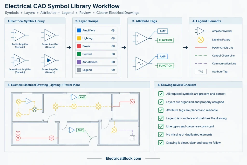
Amplifier circuit symbols DWG blocks provide reusable linework for electronics schematics and related technical drawings. A prepared symbol collection can reduce repetitive drafting while helping designers maintain a consistent visual language across diagrams, legends, and documentation sets.
The downloadable source content below should be reviewed as a CAD resource rather than treated as a complete design specification. Before using any block, confirm its graphical meaning, connection points, labels, layer behavior, and compatibility with the conventions established for the destination drawing.
Discover a comprehensive DWG file featuring a collection of Amplifier Circuit Symbols, perfect for electrical and electronics engineering projects. This CAD Block includes clear, standardized representations for various amplifier types, enabling you to design and document your circuit diagrams efficiently. Ideal for use in schematics, PCB layouts, and technical documentation, these symbols ensure precision and professionalism in your work. Fully compatible with AutoCAD and other leading CAD software, this DWG file streamlines your workflow, making it easier to integrate amplifier circuit symbols into your designs for educational, industrial, or research applications.
Please log in or register to download this file.
Using Amplifier Symbols in CAD Drawings
Amplifier symbols communicate a circuit function through simplified geometry, terminals, labels, and signal-flow cues. Their usefulness depends on more than appearance: the symbol must remain legible, connect cleanly to schematic lines, and match the terminology used elsewhere in the drawing package.
When adding a DWG block to an existing schematic, inspect its insertion point and orientation before connecting conductors or signal paths. Check whether labels are ordinary text, attributes, or separate entities. This affects how easily device identifiers and functional notes can be edited without altering the underlying symbol.

Drawing Review Reference
- Symbol meaning: Confirm that the graphic represents the intended amplifier function and does not conflict with the project legend.
- Connection points: Make sure incoming, outgoing, power, and reference connections align with the schematic linework.
- Signal direction: Use consistent orientation so readers can follow the drawing without unnecessary line crossings.
- Labels and attributes: Review identifiers, terminal descriptions, and notes for clarity and consistent formatting.
- Layers: Move geometry, text, and connection information to the appropriate project layers when necessary.
- Line appearance: Check color, linetype, and lineweight behavior in both model space and plotted output.
- Drawing units: Verify the source block against the units and insertion settings of the destination file.
- Library naming: Use a searchable block name that distinguishes the symbol from equipment layouts and physical component outlines.
Schematic Symbols and PCB Footprints Are Different
An amplifier schematic symbol expresses electrical or functional relationships. A PCB footprint represents physical pads, placement, and manufacturing geometry. A schematic block should not be assumed to contain package data or a verified footprint simply because it is used during electronic design documentation.
Likewise, an amplifier symbol is not the same as an equipment-layout block. Layout drawings may show an enclosure, module, rack position, or mounting context, while circuit drawings focus on logical connections. Keeping these resources in separate CAD library categories helps prevent the wrong block type from being inserted.
Organizing the Symbols in a CAD Library
For repeated use, store the downloaded file in a controlled symbol-library location rather than copying untracked versions between projects. A practical library record can identify the symbol category, intended drawing type, revision status, and any local drafting convention that affects its use.
Related reference topics include electrical symbol legends, schematic annotations, CAD layer management, signal-flow diagrams, PCB documentation, and block attribute workflows. Connecting these topics in the documentation system makes it easier for another drafter to understand how a symbol is intended to be used.

Final Checks Before Issuing a Drawing
Review amplifier symbols at the same plotted scale and visual conditions as the rest of the sheet. Look for ambiguous terminals, overlapping text, disconnected linework, duplicated identifiers, and inconsistent orientation. The finished schematic should be understandable from its symbols, labels, legend, and notes without relying on undocumented assumptions.
Any symbol used in formal engineering documentation should be checked against the project requirements and approved drawing conventions. A reusable CAD block improves drafting efficiency, but it does not replace circuit design review or professional verification.
Frequently Asked Questions
What is an amplifier circuit symbol DWG block?
It is reusable CAD geometry intended to represent an amplifier function in a circuit drawing or schematic. Depending on how the file was created, the block may also include text, attributes, connection markers, or layer assignments.
Can these blocks be inserted directly into an existing schematic?
They can be imported or inserted through the normal DWG workflow, but the drawing units, insertion point, layers, labels, and graphical conventions should be checked first. Editing may be needed to match the destination document.
Is a schematic amplifier symbol also a PCB footprint?
No. A schematic symbol describes circuit function and connectivity, while a footprint describes physical component geometry used for board documentation. Each resource should be selected and verified independently.
Why should amplifier symbols be included in the drawing legend?
A legend helps readers interpret symbols consistently, especially when a drawing uses project-specific graphics or abbreviations. The legend should use the same appearance and terminology as the symbols placed in the schematic.
What should be checked after inserting a CAD block?
Review its orientation, connection locations, text style, layer placement, line appearance, scale behavior, and identifier format. Also confirm that no duplicate or hidden geometry affects editing or plotting.
Leave a Reply
You must be logged in to post a comment.