
This CAD resource provides schematic diode symbols in DWG format for use in electronic and electrical drawing workflows. The symbols can support circuit diagrams, educational schematics, legends, and related documentation where clear component identification is important.
Before placing any symbol into a drawing set, review its geometry, connection points, labels, layer properties, and drawing units. A diode symbol communicates circuit function rather than the physical size or installation arrangement of a component, so it should not be treated as a PCB footprint or equipment layout outline.
Discover our comprehensive DWG file featuring Schematic Diodes Symbols, perfect for your next electrical design project. This high-quality CAD Block includes a variety of standard diode representations, making it easy to accurately illustrate circuit diagrams. Designed for seamless integration, the file is fully compatible with AutoCAD and other leading CAD software. Use these schematic diodes symbols to streamline your workflow, ensure professional presentation, and enhance the clarity of your technical drawings. Ideal for electrical engineers, students, and professionals working on electronic schematics or PCB layouts. Download now for efficient, precise drafting.
Please log in or register to download this file.
Using Diode Symbols in CAD Schematics
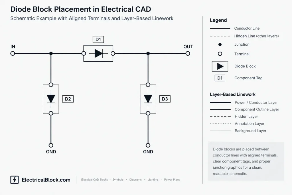
Insert the required symbol near the relevant conductors, then align its terminals with the drawing’s connection lines. Maintain consistent orientation, spacing, text style, and lineweight throughout the schematic. Where orientation affects the intended circuit meaning, verify that the symbol direction matches the design documentation before issuing the drawing.
Symbols should remain visually distinct from wires, junction indicators, equipment outlines, and annotation graphics. If the source block uses different layers or object properties from the destination file, apply the project CAD standard rather than allowing inconsistent formatting to spread through the drawing.
Recommended DWG Review Workflow
- Open and inspect: Review the downloaded file separately before copying content into an active project.
- Confirm symbol meaning: Compare each graphic with the project legend or approved symbol library. Similar diode-family symbols can represent different functions.
- Check insertion behavior: Confirm the block base point, orientation, and terminal alignment before repeated placement.
- Review drawing units: Verify that insertion does not create unexpected scaling, even though a schematic symbol is not a physical-size representation.
- Standardize properties: Move geometry to suitable layers and apply the required color, linetype, and lineweight conventions.
- Add identifiers: Use the project’s component tags, reference designations, notes, and cross-references instead of relying on geometry alone.
- Test plotting: Check that the symbol remains legible and that terminal lines, labels, and nearby conductors do not overlap.
Symbol, Footprint, and Physical Outline
- Schematic symbol: Represents electrical behavior and connectivity within a circuit diagram.
- PCB footprint: Represents pad locations and board-level placement requirements.
- Physical outline: Represents the approximate shape or space occupied by a real component or enclosure.
These drawing elements serve different documentation purposes and should not be substituted for one another. The DWG content on this page should be evaluated as schematic drafting geometry unless the source file explicitly identifies another use.
Drawing Coordination and Related References
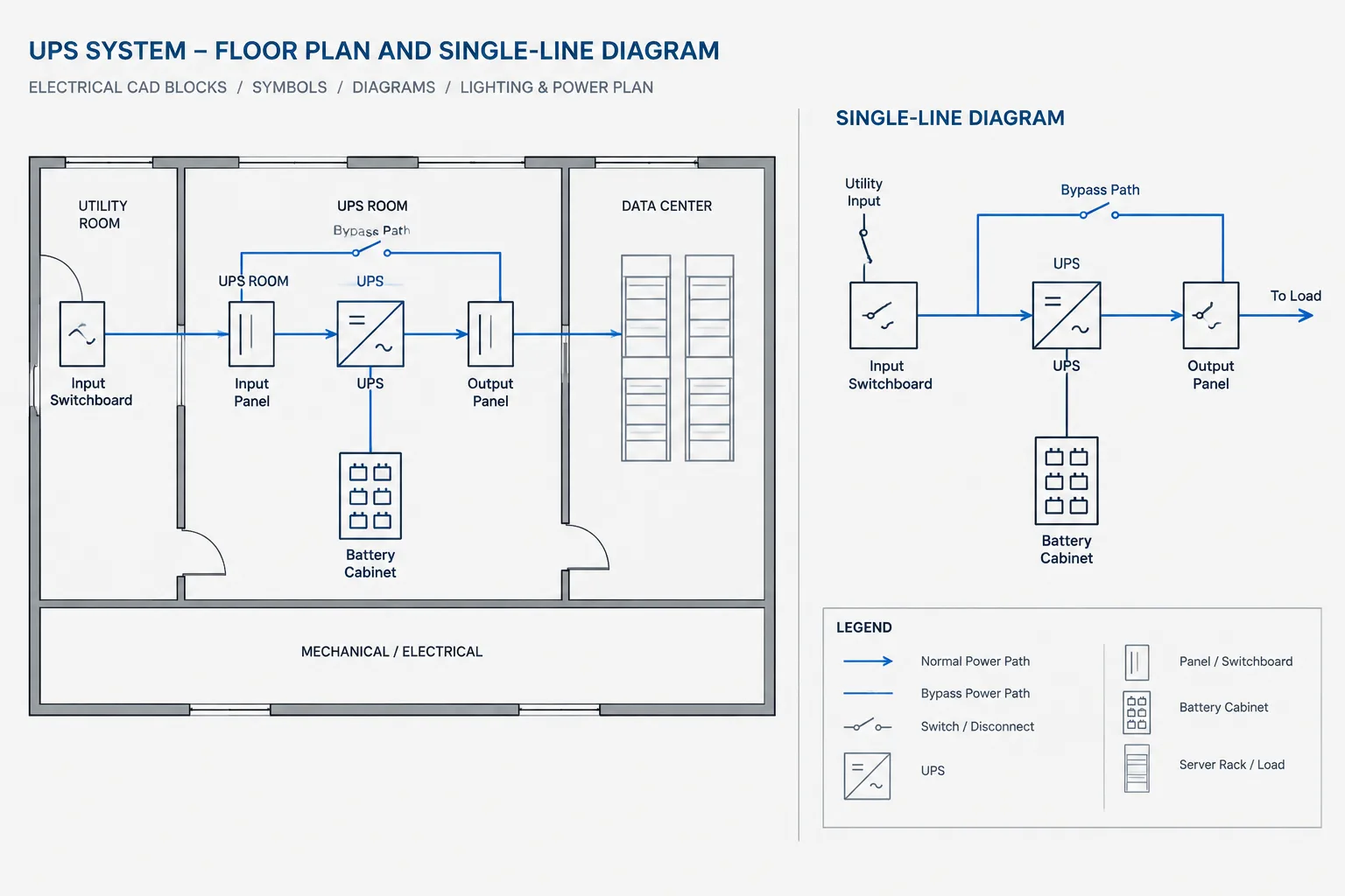
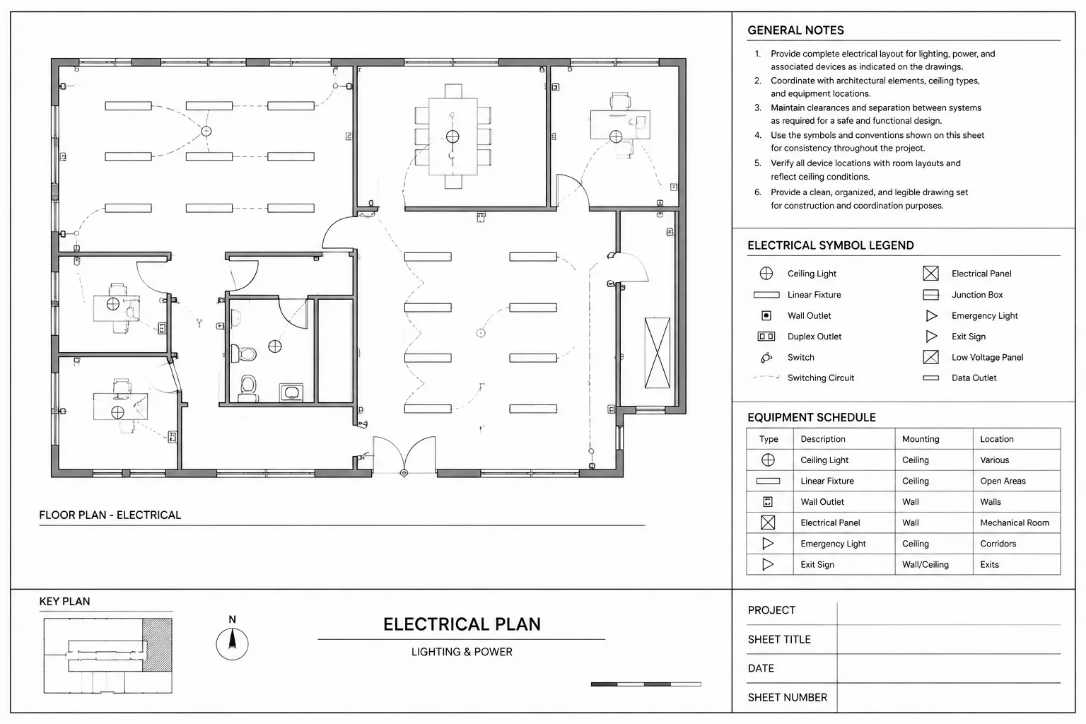
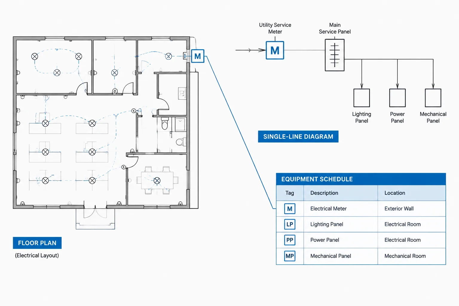
For a consistent documentation set, coordinate diode graphics with the drawing legend, general electronic symbols, connection and junction conventions, component tagging practices, and CAD layer standards. Related ElectricalBlock.com topics may include electrical CAD symbols, schematic legends, single-line-diagram concepts, wiring diagram conventions, and block-library organization.
Final symbol selection and circuit interpretation should be checked against the project’s approved documentation and design requirements. A reusable CAD block improves drafting consistency, but it does not independently verify circuit operation, component suitability, or compliance.

Frequently Asked Questions
What does the DWG file contain?
The source description identifies a collection of schematic diode symbols supplied as CAD block content. Open the file and inspect the individual graphics to determine which diode representations are included.
Can these symbols be used as PCB footprints?
No assumption should be made that schematic graphics are PCB footprints. A footprint requires verified pad geometry and component-specific package information, while a schematic symbol primarily communicates circuit function and connectivity.
Why should each diode symbol be checked before use?
Diode-family symbols can have similar geometry while representing different functions. Checking the symbol against the project legend helps prevent incorrect identification, orientation, or labeling.
Should the symbols be placed on a dedicated CAD layer?
Using an appropriate symbol or component layer can make editing, plotting, and visibility control easier. The exact layer name and properties should follow the destination drawing’s CAD standard.

Is it safe to scale a schematic symbol?
A schematic symbol does not normally represent physical component size, but its plotted size still affects readability. Adjust it only as needed to match the drawing’s established symbol and annotation conventions, while checking terminal alignment afterward.
Should the block be exploded after insertion?
Keeping a symbol as a block generally supports consistency and easier replacement. Explode it only when the documentation workflow requires editable geometry, and verify that layers, attributes, and connection points are not disrupted.
How can diode symbols remain clear in a crowded schematic?
Use consistent spacing, avoid overlapping labels, align conductors cleanly with terminals, and provide component identifiers. Junctions and crossing conductors should also follow one consistent graphic convention throughout the drawing.
Leave a Reply
You must be logged in to post a comment.